Finally finished the PCB design of the pinball IO board. It did cost me more time as expected to squeeze all the tracks on the board. I just send the design to Dirty PCBs to be manufactured.
The pinball IO board primarily function is to control coils and LEDS, and the read sensors and switch. Likely for the firepower pinball, I also use the board as a central controller. That machine does not have a DMD or matrix led display, so the board would be sufficient. Alternatively a Raspberry-pi as master controller is also still a good option.
Board
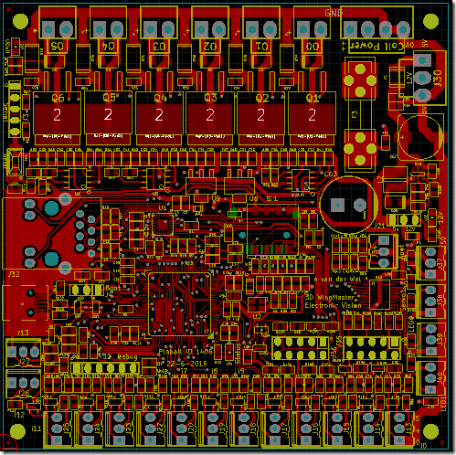
Below you can see the final pcb. It is a double sided board with a mix of SMD and through hole parts. All components are mounted on top side, except one. The surface mounted micro-sd connector has to be placed on the bottom side due to lack of space on top.
The pcb ended up as 10x10cm (4x4inch). This is a standard and cost effective size of PCB available at a lot of Chinese vendors. Most resistors and capacitors are 0805 size. I choose 0805, because I had already a set of these at home, and they are still good size to handle. Possible in hindsight I should have used 0603 instead of the 0805 to save some space.
All connectors are through hole. These are stronger and more cost effective then surface mount versions.
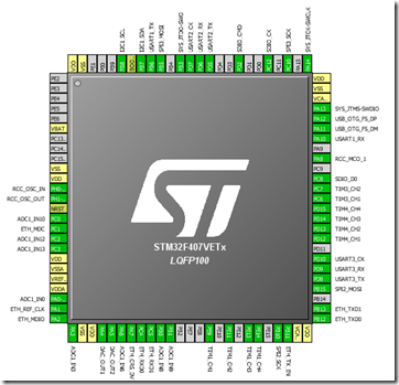
The picture shows the top silkscreen and top traces. Both the top and bottom copper layers are very crowded around the U3, the 100pin processor. On the end had a hard time squeezing the last traces in.
The most critical component on the pcb is U1: the QFN package of the LAN8720 Ethernet phy. I ready hope I manage to solder the fine pitch QFN part with all its hidden pads to the board
Originally I planned to have 8 coil outputs and 16 digital inputs. But that did not fit on the 10x10cm pcb and had to drop some. The PCB ended up having 6 coil drivers and 14 switch/sensor inputs. This is still very good ratio. For a Firepower pinball you only need 4 or 5 PCBs, depending if the master can handle coils or not.
In some way I always end up with boards that have to many features. Also this board. If I would have limited the board features to only coil outputs and sensor inputs, the routing of the board would have been so much easier. But no, I like to put more features on it. And a lot of times never use all these extra features…..
Features
I will never learn. So the board ended up with the following features:
- A 100baseT Ethernet interface. The primarily control interface
- A mini usb connector. This can be used to programming and control.
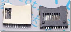
- A micro-sd card connector. Used to store log files and music and other data.
- 6 outputs with high voltage (upto 50v) & high current outputs for coil and motor.
- 14 digital inputs. They can supply either a 5v or 12v rail to feed the sensors.
- 2 analog outputs for either audio or other controllable voltages.
- 2 LED chain outputs controlling a row of programmable WS2812 RGB leds.
- 2 Servo outputs
- a 5v and a 3.3v digital IO connector supporting various interfaces type like I2C, UART, SPI and general IO.
- a voltage boost from 5v to 12v.
- a ARM Debug header
- Uart interface for debug or other purposes.
- A 4 bit dip switch to set the Node address.
- buffer capacitors on the high voltage and 5v rails.
- Glass fuse in the high voltage (0..50v) rail . Poly fuse in the 5v rail and sensor power rail.
- Couple of power rail and status leds.
- And a very usefull reset button.
CPU
The CPU choice has not changed. I am still using the STM32F407VGT6 . Originally I planned to make a excel sheet to select the pin usage of the processor. But then I came across the program STM32CubeMX from ST. Very useful. This program allows the selection of peripherals you like to use. It right away marks other interfaces that are not accessible any more, because the pin is in use. So it is a bit of trying out till you have the correct combinations.
And also very nice is that is can create all the header files needed to initialise the CPU. This even inclues FAT filesystems, TCP/IP stacks and even FreeRTOS. I still have to try out this part.
Coil drivers
The coil/motor outputs are capable of a lot of amps and volts. The IRF3710ZS Fets are good for 100v and 59A. Current limiting factor will be the PCB tracks and fuse rating. A glass fuse protects the board and coil from overheating. The voltage is limited by the 63v elco used as buffer, and the track to track spacing on the PCB.
Each coil current is measured by the processor, so the CPU can disable the outputs on a high current. I also going to try if a controlled output current is possible. In that case instead setting a PWM percentage like all other boards, you can set the coil current. Coil current has a direct relation to coil power and heating.
The fets are driven in saturation by a gate buffer chip IR4427S. In that way the heating of the fets will be minimised. To drive the the fets in saturation a gate voltage >8v is needed.
PSU
Originally I have planned a 12v input voltage, and step that voltage down to 5v and 3.3v for the led and logic. Sadly the inductors needed are quite large to create the 2 to 3 ampere needed on the 5v rail to feed all the ws2812 leds.
Therefore now the board is fed with 5v and a boost converter is used to create a 12v rail. The 12v is used to the FET drivers and optionally to feed the input sensors. The sensor can also be feed directly from the 5v rail, jumper selectable.
The 5v is directly fed to the leds and servos, after passing a poly fuse and buffer capacitor. With two AMS1117-3.3V linear regulators the 3.3v rails for the PHY and CPU are generated. I used 2 because the exact current needed by the Ethernet phy and CPU was quite uncertain .
Some parts
Mini-USB. I liked to have micro-usb, but could not find a nice SMD version.
Micro SD connector. This is a push/pull version
Schematic/ PCB design
I used Kicad as cad tool. I was very very pleasant surprised that Kicad was working so well. I uncounted hardly any problems with the program. It was very stable and usable. Lot of people complain about the user interface and library management, but that was not my experience at all. You have to set up the libraries you like to use, and need to lean the key presses. But thats it. I also use Altium quite a lot for PCB design. Altium has much more features, but if you look what you actually need and use, then kicad is just as good! In kicad to tend to need less keypresses as in Altium for most functions. E.g. start a new track is the most used function during PCB design. In altium this is p t (2 keypressses) in kicad x (1 press). After a day work that saves you 100’s or even 1000’s of presses. Altium is around usd$7000? per user, and Kicad is free without limits. Kicad is now so mature, i don’t see any need for expensive programs like Altium or Eagle.
As a base set of symbols and footprint i used http://smisioto.no-ip.org/elettronica/kicad/kicad-en.htm a lot. Also very nice is the integration with git. This allows to load footprints from a central GIT repository! Very nice. In the end I had copied most footprints to my own library. In a lot of cases the silkscreen is over the pads what is not very useful. Also a lot of pads are minimal in size that I liked larger for a more robust design.
The only thing that does not work yet in my setup is the 3d view. I have not figured out what path to set. But I did not miss the 3d view to much. In Altium this is also more a gimic. The primary use of 3d I think it to be able to save a 3d model of the pcb. That model then can be loaded in a 3d design program to check if it fits in the housing.
Some things are a bit strange in kicad: For example in the PCB program has different canvas : F9 and F11 and even F12 (never used F12), that each has its own set of features and menu’s. Caught me out a few times. Also there are a lot of buttons on the screen that you never need to use, and could be removed to have more space for the PCB itself.
To position parts, I used F9. If you select a part in the schematic, it is highlighted in the PB and other way around. This help very much in placement . All the track wrok I did in F11, because that has much better track colouring and of course the track pushing option.
For quite a while I did not know it that the kicad version I used had a push and shovel router! That is only available in F11 and when you enable it in the menu. Should be default on. But that is a very powerful option to get an extra track in a tight space. It has some unpolished aspects, like breaking tracks into many segments if going around a pad. But lucky it cleans up a lot of that if you push nearby track a bit!
In the PCB program I mainly use the following keys:
- x lay a track
- v add via or swap layer
- e edit part or router setting
- delete a track
- w and shift w to change track width. (I should change this this w and q)
I still need to find a way to change grid spacing with key presses.
I use a 10mill grid to place parts, and 1 mill grid for tracks. Track widths used are 0.25mm 0.5mm 1mm 1.5mm and 2mm
Board population
Besides the nasty QFN part has the board lots and lots of other parts. It will be fun to load up the board with this massive amount of passives. Now I have to be careful. I am reading way to many web sites about pick and place machines, and they look quite easy to make. Do not start another project….
To help with solder paste placement, I also ordered in a stencil at the same Dirtypcb manufacturer. To solder the pcb i bought a small toaster oven. Sadly my wife saw it and confiscated the oven for the kitchen duty :-<
Also also looked into making my own stencils out of aluminum cans (see http://www.popsci.com/article/diy/build-diy-soldering-stencil-out-soda-can ) , and that does not look too complex. But not this time. I need to reduce the number of uncertainties to make progress. The number of uncertainties/first times is already way to high (kicad smd design, arm processor, arm toolchains, qfn packages, paste and refow soldering, 50mhz clocks, freertos etc etc)
PCB vendors
To find a PCB vendor with a good price the website http://pcbshopper.com/ is very useful. This searches with your given pcb specifications several vendors for pricing.
Now waiting for the pcbs to come back….


